Introduction: The Infrastructure Shift in Open-Source ASIC Deployment
The rapid expansion of edge computing nodes, university STEM research clusters, and enterprise-grade micro-data centers has fundamentally changed hardware procurement requirements. Historically, open-source solo mining hardware relied exclusively on single-band 2.4G Wi-Fi modules designed for domestic hobbyist environments. For enterprise IT directors and regional technology distributors deploying hundreds of nodes within high-interference server racks, single-band wireless connectivity introduces packet loss, elevated latency, and severe operational vulnerabilities.
DigLucky bridges the gap between open-source flexibility and industrial-grade reliability. As a primary source manufacturer with research and development operations in Beijing and advanced SMT production lines in Shenzhen, we engineer custom PCBA solutions that incorporate robust dual-band Wi-Fi (2.4G/5G) and physical RJ45 Ethernet interfaces directly onto high-efficiency ASIC mainboards. This white-paper details our engineering methodology, multi-chip performance metrics, and transparent B2B supply chain protocols.
Engineering & Supply Chain Deep Dive: Integrating Dual-Band Wi-Fi and RJ45
Deploying computational hardware in institutional facilities demands dual-path connectivity options to ensure uninterrupted uptime. Standard open-source layouts lack the physical board space and circuit protection required to run high-speed network controllers alongside high-frequency hash chips.
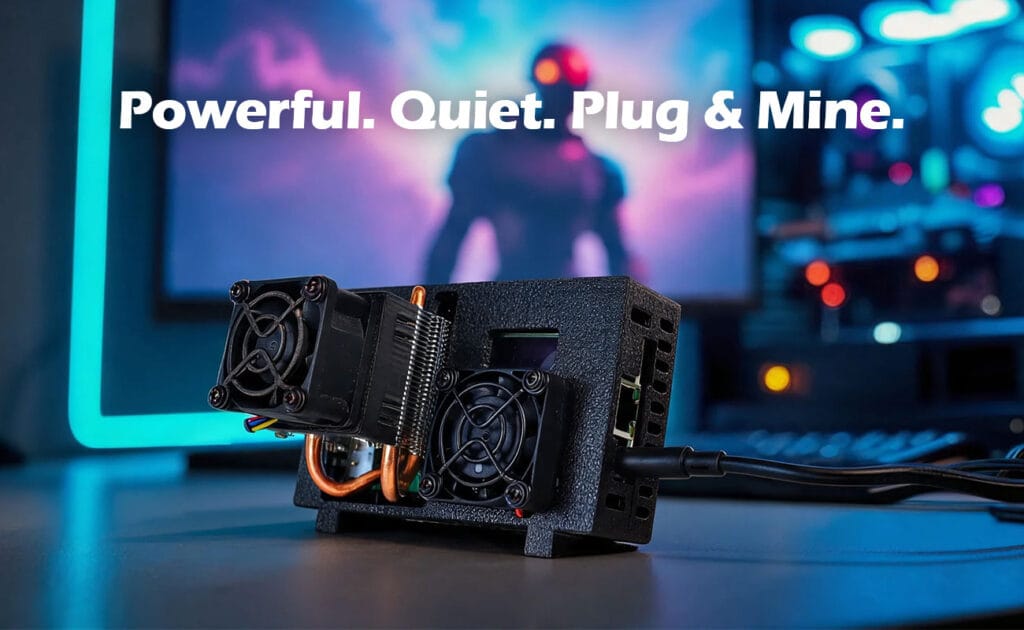
Our engineering team redesigned the core PCB layout to isolate the power delivery planes from the network transceiver modules. By embedding an enterprise-grade Ethernet controller and a dual-band 2.4G/5G wireless transceiver, our hardware supports both ultra-stable wired infrastructure routing and flexible wireless management.
DigLucky Source Factory Standards vs. Alibaba Middlemen Risks
Navigating the global hardware supply chain involves critical structural risks. Institutional buyers frequently encounter unverified traders on online marketplaces who compromise hardware integrity for short-term margins.
- Silicon Integrity: DigLucky strictly utilizes 100% new, factory-fresh silicon wafers (such as the BM1370 and BM1368) sourced directly from Tier-1 semiconductor channels. Middlemen and brokers frequently utilize desoldered, heat-stressed secondary market chips salvaged from retired industrial rigs, leading to premature thermal degradation.
- Quality Assurance & Burn-In: Every PCBA produced in our Shenzhen facility undergoes automated optical inspection (AOI) followed by a mandatory 48-hour full-load burn-in protocol under monitored thermal stress. Traders dropship untested units straight from unverified assembly workshops, resulting in high Dead-on-Arrival (DOA) rates and costly field returns.
- Financial Security: We protect B2B cash flows through corporate T/T Wire Transfers settled directly via institutional banking channels. Unverified suppliers rely on high-risk retail payment gateways with strict volume caps and zero legal recourse for cross-border commercial disputes.
Enterprise Specifications & Multi-Chip Financial Modeling
DigLucky has achieved mature mass production across single-chip, dual-chip, and quad-chip topology series, offering scalable computing power and power efficiency profiles tailored to specific B2B deployment vectors.
| Series & Model | ASIC Topology | Network Interface Configuration | Target Efficiency (J/TH) | Packaging & Logistics Format | Primary B2B Deployment Vector |
| Luckyaxe 101 Series | Single BM1368 | RJ45 + 2.4G/5G Dual-Band Wi-Fi | ~15–18 J/TH | 20 Units / Master Carton | Regional Tech Distribution, STEM Labs |
| Luckyaxe 201Series | Dual BM1370 | RJ45 + 2.4G/5G Dual-Band Wi-Fi | ~15–16 J/TH | 10 Units / Master Carton | Micro-Container Data Centers, White-Label OEM |
| Luckyaxe 401 Series | Quad BM1370 | RJ45 + Dedicated 5G Wi-Fi Module | < 15 J/TH | 10 Units / Master Carton | High-Density Compute Racks, Enterprise R&D |
DigLucky Factory Insight: Quality Control and SMT Excellence
Our manufacturing floor in Bao’an District, Shenzhen, operates under strict ISO-aligned production management. The fabrication of custom PCBA miner units with integrated RJ45 and dual-band Wi-Fi modules requires precision surface-mount technology (SMT) placement.
- Solder Paste Deposition: Automated stencil printers apply lead-free solder paste with micrometer precision to accommodate fine-pitch network controller ICs.
- Reflow Profiling: Multi-zone thermal reflow ovens ensure flawless intermetallic compound formation across all hash chips and interface modules, preventing micro-fractures under thermal expansion.
- Telemetry Calibration: Each unit is flashed with optimized AxeOS firmware, calibrating core voltage, frequency curves, and real-time screen telemetry prior to final casing assembly.
Common Supply Chain & OEM Pitfalls
Procuring custom hardware from inexperienced overseas suppliers exposes institutional buyers to severe financial and operational hazards:
- Hidden NRE Surprises: Unverified brokers quote low initial unit costs while concealing Once-Off Engineering (NRE) fees for custom PCB traces, resulting in unexpected budget overruns.
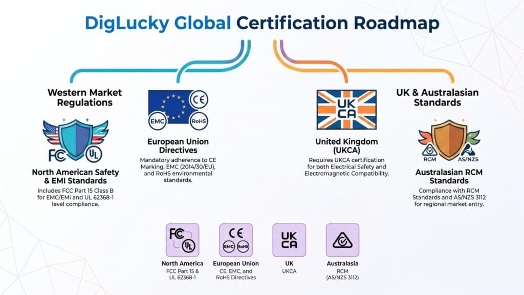
- Customs Clearance Delays: Inadequate compliance documentation causes prolonged port inspections. DigLucky units are fully certified to global standards, ensuring frictionless clearance.
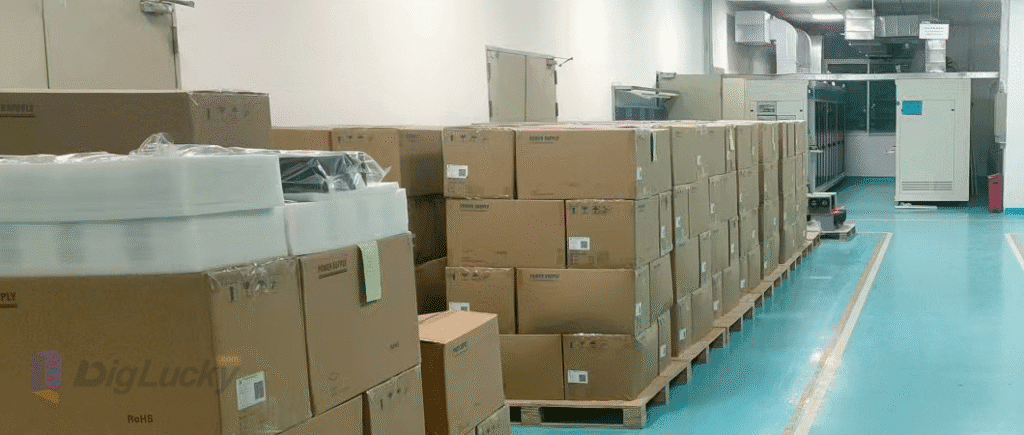
- Logistical Damage: Incompatible packaging leads to crushed heatsinks during transit. We mitigate this by boxing all hardware in reinforced Master Cartons with custom high-density polyethylene foam inserts.
Frequently Asked Questions (Diagnostic & Compliance Focus)
Q1: What is the minimum order quantity (MOQ) for custom PCBA miner OEM modifications such as integrated RJ45 and custom solder mask colors?
A: For deep PCB layout customization, custom shell branding, and specialized network module integration, our standard Minimum Order Quantity (MOQ) is 500 units, with an estimated production lead time of 6 weeks.
Q2: How are bulk wholesale orders packaged and transported globally?
A: All wholesale inventory is systematically packed into reinforced Master Cartons (configured in 10 or 20-unit quantities depending on the model footprint). We support global logistics via direct DAP Air Freight or EXW Shenzhen terms coordinated with your designated freight forwarder.
Q3: What payment methods are accepted for institutional B2B procurement?
A: To ensure maximum security, compliance, and large-volume liquidity, all corporate orders are processed strictly through secure T/T Wire Transfers. Retail payment methods like PayPal are disabled for B2B wholesale transactions.
Q4: Do your hardware units comply with international electrical safety and import standards?
A: Yes. All production lines adhere to stringent regulatory benchmarks, and complete compliance documentation is provided during the Proforma Invoice (PI) stage.
Ready to Start Your Project?
Get a factory-direct quote for your B2B project, or shop our B2C store for the best prices.