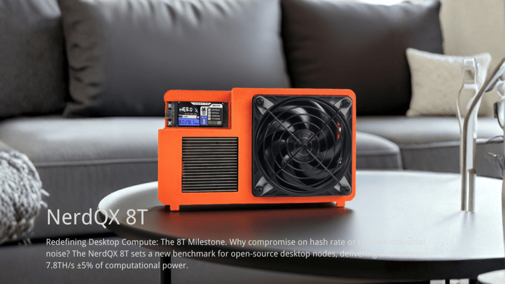
The transition from generalized computing to specialized silicon dictates the evolution of the Bitcoin network. For B2B procurement managers, university lab directors, and hardware syndicates sourcing decentralized edge nodes, understanding the fundamental architectural differences between Field-Programmable Gate Arrays (FPGAs) and true Application-Specific Integrated Circuits (ASICs) is critical.
In the specific context of the SHA-256 algorithm, customized ASIC chips (such as the 5nm BM1370) possess an absolute advantage, completely crushing generic FPGA architectures in both computational hashrate density and J/TH (Joules per Terahash) power efficiency. This guide unpacks the engineering rationale behind this discrepancy, ensuring your next hardware procurement cycle prioritizes stable, scalable, and efficient silicon.
Engineering Overview: FPGA vs. ASIC Architecture
To understand why ASICs dominate SHA-256 cryptographic hashing, we must analyze the silicon at the logic-gate level.
- FPGA (Field-Programmable Gate Array): FPGAs are highly flexible, integrated circuits configured by the consumer after manufacturing. They consist of a matrix of configurable logic blocks (CLBs). While they can theoretically mine Bitcoin by being programmed with the SHA-256 algorithm, the physical overhead of routing logic and programmable interconnects wastes massive amounts of physical die space and power.
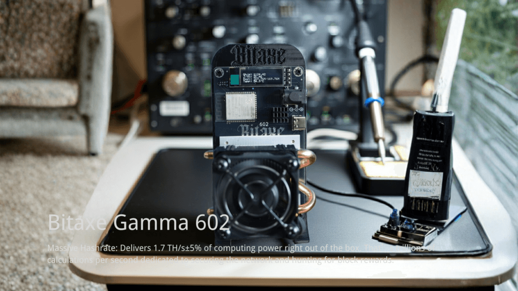
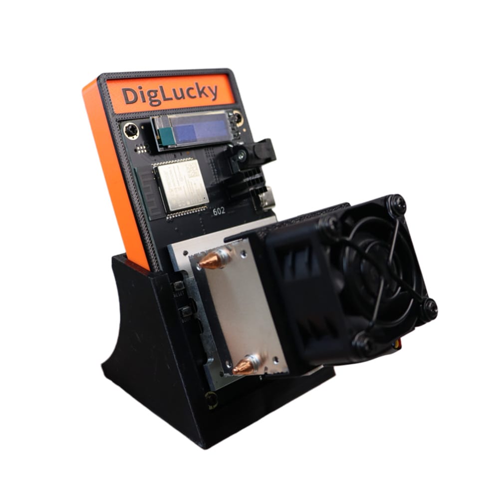
- True ASIC (Application-Specific Integrated Circuit): An ASIC, such as the Bitmain BM1370 utilized in the DigLucky Bitaxe Gamma 602, is hardcoded at the foundry level. The silicon is permanently etched to perform exactly one mathematical function: SHA-256 double-hashing. By stripping away all generalized logic gates, ASICs pack millions more hashing cores into a smaller footprint, drastically reducing the electrical resistance and logic delay.
Hardware Specifications
| Specification | Typical FPGA Node (e.g., VU9P) | True ASIC Node (Bitaxe Gamma 602) | True ASIC Array (NerdOctaxe 12T) |
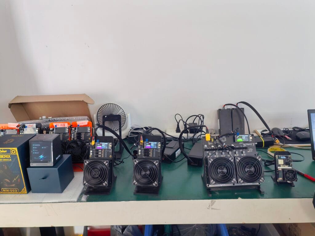
| Silicon Architecture | Reprogrammable Logic Gates | Hardcoded 5nm SHA-256 Silicon | 8x Hardcoded 5nm SHA-256 Array |
| Hashrate Density | ~3 – 10 GH/s | 1.8 TH/s (1,800 GH/s) | 12.0 TH/s (12,000 GH/s) |
| Power Consumption | ~75W – 150W | ~35W | ~200W |
| Efficiency (J/TH) | > 10,000 J/TH | ~19.4 J/TH | ~16.6 J/TH |
| Primary Use Case | Multi-algo Altcoin Hashing | High-Efficiency BTC Solo Mining | High-Density Edge Node Deployment |
Step-by-Step SOP: Evaluating Hardware for Procurement
When sourcing mining hardware for institutional or distribution purposes, follow this engineering protocol to avoid obsolete or inefficient architectures:
- Verify the Silicon Foundation: Audit the Bill of Materials (BOM). Ensure the device utilizes dedicated SHA-256 silicon (e.g., BM1366, BM1370) rather than generic multi-purpose processing units.
- Calculate the J/TH Efficiency Ratio: Divide the baseline power consumption (Watts) by the output hashrate (Terahashes). A modern B2B deployment must operate under 25 J/TH to remain viable.
- Audit the Power Delivery Network (PDN): Verify that the PCBA is equipped with industrial-grade voltage regulation capable of sustaining continuous DC loads without fluctuating.
- Confirm the Telemetry Subsystem: Ensure the hardware supports integrated microcontrollers (like the ESP32-S3) running reliable open-source firmware (such as AxeOS) for real-time monitoring.
Technical Validation: DigLucky Factory Standard vs. DIY Clone Risks
DigLucky Factory Standard
DigLucky utilizes automated SMT (Surface-Mount Technology) assembly lines in Shenzhen to mount 5nm BM1370 ASICs onto custom, high-density PCBAs. By employing solid-state capacitors and rigorous trace impedance control, our power regulation maintains absolute stability at 5V/8A inputs. Every unit undergoes a strict 48-hour thermal burn-in protocol in a climate-controlled chamber to guarantee zero thermal throttling before global DAP shipment.
Generic DIY Clone Risks
Unverified DIY assemblers often source secondary-market chips and hand-solder components onto unoptimized FR4 boards. These clones frequently suffer from poor thermal pad application, leading to uneven heat dissipation. Without factory-level voltage calibration and burn-in testing, these boards face high failure rates, unstable PDNs, and rapid silicon degradation when subjected to 24/7 continuous loads.
Common Mistakes in Procurement
- Prioritizing Flexibility over Density: Purchasing FPGAs under the assumption that “multi-algorithm flexibility” is safer. For Bitcoin (SHA-256), the density disparity renders FPGAs mathematically obsolete.
- Ignoring the J/TH Metric: Focusing solely on the device cost without calculating the ongoing electrical OPEX.
- Sourcing from Middlemen: Relying on trading companies that lack SMT production lines, resulting in zero quality control transparency and inflated RMA rates.
FAQ & Troubleshooting
Q: My BM1370 ASIC node is reporting high hardware error rates in the AxeOS WebUI. Is the silicon failing?
A: Not necessarily. High error rates are frequently tied to voltage instability rather than silicon degradation. Use a multimeter to measure the input voltage directly at the board terminals. If it drops below 5.0V under load, your power supply is insufficient. Upgrade to the factory-certified 5V/8A (40W) switching power supply.
Q: Why does my device temporarily throttle hashrate even in a cool room?
A: Check your AxeOS thermal logs. The internal core temperature of the ASIC dictates the PWM fan response. If the heatsink mounting pressure is uneven (a common issue in DIY kits, but prevented by DigLucky’s automated assembly), thermal transfer fails. Ensure the thermal interface material is intact and the PWM fan curve is set to aggressive in the WebUI.
Q: Can I re-flash an ASIC to mine Scrypt coins like Litecoin?
A: No. True ASICs possess hardcoded logic pathways at the silicon foundry level. A BM1370 chip is physically incapable of performing Scrypt algorithms. You must procure a dedicated Scrypt ASIC (e.g., the Lucky Miner LG07 series) for that network.
Factory Insight: SMT Assembly and Burn-In Validation
At DigLucky’s Shenzhen facility, quality control is not an afterthought; it is integrated into the manufacturing architecture. Our automated SMT assembly lines utilize highly precise pick-and-place robotics to mount the sensitive 5nm ASIC silicon, ensuring micron-level accuracy that manual soldering cannot achieve. Following PCBA fabrication, 100% of our production batch enters a 48-hour high-load burn-in testing phase. We continuously monitor thermal telemetry and voltage stability under peak hashing frequencies to weed out infant mortality failures, ensuring distributors receive zero-defect Master Cartons.
B2B Procurement Section
For global hardware syndicates and educational institutions, procuring the right architecture dictates your operational margin. Sourcing FPGAs for SHA-256 education or node deployment is a misallocation of capital. By partnering directly with the DigLucky Source Factory, you secure Tier-1 Master Box pricing on true 5nm ASIC desktop nodes (like the NerdQX 8T or NerdOctaxe 12T). We eliminate intermediary markups and deliver fully CE/FCC-certified, OEM-ready hardware via reliable DAP air freight logistics.
Final Recommendations
To maximize your infrastructure ROI, restrict SHA-256 deployments exclusively to true ASIC architectures. The BM1370 silicon provides the optimal balance of acoustic compliance, power efficiency, and hashrate density for localized edge environments.
Start Your Project Today
Submit your requirements (even if they’re just an idea) and our B2B team will contact you within 48 business hours.